• 1

    ..

  • 2

    ...

  • 3

    ...

Saturday, 26 October 2013

About MAX7219 LED Display Dot-matrix Display Driver - Data Format - Register Map - Programming


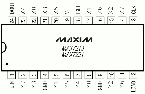
                The MAX7219 chip from maxim is a powerful serial input/output common-cathode display driver that interfaces microcontroller to 7-segment numeric LED displays of up to 8 digits and a 8x8 dot-matrix displays. The pindiagram of MAX7219 is (for MAX7221, pin 12 is CS_bar)

MAX7219
Typical application circuit is


Many MAX7219 can be cascaded serially through DOUT pin of one IC to DIN of the another, but with common clock and load connections. 

        It needs only 3 wires to interface with the microcontroller or microprocessor namely, CLK, LOAD and DIN. It has a build-in BCD (binary code decimal) decoder and a brightness control. It is easy to enable or disable the BCD decoder through the registers. Although the main function is to drive the 8-Digits seven segment LED display but because it also capable to drive an individual LED segment i.e. segment A to segment G and DP (decimal point), by disabling the decoder.

         The MAX7219 chip has 16-bit registers divided into two ADDRESS and DATA each of 8 bit size. The data format for programming is
at the negative edge of CLK, the DIN appears at DOUT for cascading

                In order to send a command to the MAX7219 chip, first we need send the 8-bits address and next we send the 8-bits data. It uses D8-D11 as address to map 14 registers. The register map is //               

           //Max7219 Command registers Address
               DECODE         0x09      // Decode mode register Address
               INTENSITY     0x0A      // Intensity register Address
               SCAN_LIMIT   0x0B      // Scan limit register Address
               SHUTDOWN   0x0C      // Shutdown register Address
               DISPLAY_TEST  0x0F     // Display test" register Address
               NOP  0x00
               D0  0x01
               D1  0x02
               D2  0x03
               D3  0x04
               D4  0x05
               D5  0x06
               D6  0 x07
               D7  0x08

          The data byte should be proceeded by the address byte.
       The segment current is set by an external resistor (Rset) connected to pin 18 and VCC. The intensity can be controlled by software using Intensity register, setting values 1 (min) to 15 (max).

          The Shutdown mode turns off all segment drives if its data is 0x00 and normal op if 0x01.

          The Display test mode turns on all segment drives if its data is 0x01 and normal op if 0x00.

        The Decode register is used to enable BCD decoder for the digits. the values are NONE=0x00,  D0=0x01,  D0-D3=0x0F,  D0-D7=0xFF

        The Scan limit register is used to set the number of used digits. 

      The same principle is also apply to other important MAX7219 chip commands such as activate from the shutdown mode (normal operation), use BCD decode (code B) mode, scanning limit (scanning digit 0 to 7), and adjusting the seven segment LED digit intensity please refer to the Maxim MAX7219 datasheet for the complete explanation.


          Comming soon: Interfacing MAX7219 with AVR for 7seg LEDs & later 8x8 dot matrix displays... Stay Tuned. Dont miss it.


If you have any doubts/need any clarification plz let us know your views via comments or mail us through   admin@elecdude.com
This helps us to do much more better.

Thankyou.

Thursday, 24 October 2013

FONT MAP HEADER FOR GLCD DOT-MATRIX DISPLAYS - AVR PIC

        The GLCDs & Dot-Matrix displays cannot directly display ASCII characters. And needs to be displayed bit-by-bit or byte-by-byte in specific manner to display the required character. Here are the font memory map that resides in program memory of the controller & then read and displayed sequentially to create a particular ASCII character.


        Font Map or font header file for GLCD & Dot-Matrix displays for AVR microcontrollers, also supports PIC, etc (GCC Complier). The font display sizes are 5x7 & 5x8 pixels.

        The header file contains the format for reading & displaying the ASCII character.

Click to download the font header file.
Font_5x7.h   Specially for 8x8 Dot-Matrix Display using 7219
Font_5x8.h  Specially for GLCD from Osama's Lab
Font_5x7.h   for GLCD


If you enjoyed this post plz let us know your views via comments.
This helps us to do much more better.
Thankyou.


Saturday, 5 October 2013

Image Processing in VHDL - Adding Images VHDL code


      Often image processing in HDL (verilog/VHDL) is a bit complex task when it comes for simulation & implementation in real environment where the image has to be converted into a HDL compatible form.

     We have already seen how to convert an image into text and to reconstruct image back from a text file [ Click here to view it. ] and also how to process them in Verilog. Now let us see how to do it in VHDL.


VHDL Image Processing ElecDude.com

        In previous postings, VHDL file read write operations & datatype conversions have been described.  

The steps involved in image processing in VHDL are
  1. Image to text in Matlab
  2. Read text in VHDL
  3. Convert real value (read from text) into bit vector
  4. Process the bit vector & get required result
  5. Convert the resultin bit vector to integer (decimal)
  6. Write to output text file
  7. Reconstruct output image from output text file
      The code is organised into different processes such as Clock generator, read and write. The clock generator produces the clock signal for the TB & DUT.

      The reading process reads the text file, converts it to bit vector and assigns to the input ports of DUT i.e., Image Adder. Once the EOF of the input text file is reached, the endoffile signal is set indicating the task completion.

     The write process gets the result vector, converts it to integer & writes to text file until the endoffile signal is in state '0'.


Read Process:
                 if (not (endfile(infile) or endfile(infile2)) ) then --checking the "END OF FILE" is not reached.
                    readline(infile, inline);
                    read(inline, dataread1);
                    d1 <=integer(dataread1);
                a <= CONV_INT2STDLV(d1,8);
                    readline(infile2, inline2);
                    read(inline2, dataread1);
                    d2 <=integer(dataread1);
                b <= CONV_INT2STDLV(d2,8);
        else   
                a<=x"00";
                b<=x"00";
                endoffile <='1'; --set signal to tell end of file read file is reached.
        end if;


Write process:
         if(endoffile='0') then --if the file end is not reached.
            intt <= CONV_STDLV8bit_2INT(sum);
            if(linenumber>3) then
            write(buff_out, intt); 
            writeline(outfile, buff_out);-- write line to output_image text file.
            n <= n+1;
          end if;   
            linenumber <= linenumber + 1;
         end if;

The simulation output is....


VHDL image processing ElecDude.com

Click here to download the VHDL files    IMADDER.vhd         TestBench.vhd

Click here to goto VLSI articles.


If you enjoyed this post plz let us know your views via comments.
This helps us to do much more better.
Thankyou.

VHDL File I/O - File read write code example

     Here we present the VHDL File I/O syntax and examples.

     This is very useful in handling file i/o for processing signals, images into VHDL codes.

VHDL ElecDude.com


VHDL File operations:

  • File open
  • File read/write
  • File close

Friday, 4 October 2013

VHDL Real/interger to STD Logic Vector and STD Logic vector to Integer datatype conversion code example

     Here is a simple function for converting integer number to STD logic vector and vice versa. The width can be easily adjusted upto 32 bits (max size of integer number).

     This is very useful in handling file i/o for processing images into VHDL modules.

VHDL ElecDude.com


STD LOGIC VECTOR to 8 bit INTEGER:

serial communication protocol I²C vs SPI: is there a winner?

                      Serial Communication Protocol                                

 I²C vs SPI: is there a winner?

Let’s compare I²C and SPI on several key protocol aspects:

- Bus topology / routing / resources:
I²C needs 2 lines and that’s it, while SPI formally defines at least 4 signals and more, if you add slaves. Some unofficial SPI variants only need 3 wires, that is a SCLK, SS and a bi-directional MISO/MOSI line. Still, this implementation would require one SS line per slave. SPI requires additional work, logic and/or pins if a multi-master architecture has to be built on SPI. The only problem I²C when building a system is a limited device address space on 7 bits, overcome with the 10-bits extension.
From this point of view, I²C is a clear winner over SPI in sparing pins, board routing and how easy it is to build an I²C network.

- Throughput / Speed:
If data must be transferred at ‘high speed’, SPI is clearly the protocol of choice, over I²C. SPI is full-duplex; I²C is not. SPI does not define any speed limit; implementations often go over 10 Mbps. I²C is limited to 1Mbps in Fast Mode+ and to 3.4 Mbps in High Speed Mode – this last one requiring specific I/O buffers, not always easily available.

- Elegance:
It is often said that I²C is much more elegant than SPI, and that this last one is a very ‘rough’ (if not ‘dumb’) protocol. Actually, we tend to think the two protocols are equally elegant and comparable on robustness.
I²C is elegant because it offers very advanced features – such as automatic multi-master conflicts handling and built-in addressing management – on a very light infrastructure. It can be very complex, however and somewhat lacks performance.
SPI, on the other hand, is very easy to understand and to implement and offers a great deal of flexibility for extensions and variations. Simplicity is where the elegance of SPI lies. SPI should be considered as a good platform for building custom protocol stacks for communication between ICs. So, according to the engineer’s need, using SPI may need more work but offers increased data transfer performance and almost total freedom.
Both SPI and I2C offer good support for communication with low-speed devices, but SPI is better suited to applications in which devices transfer data streams, while I²C is better at multi master ‘register access’ application.
Used properly, the two protocols offer the same level of robustness and have been equally successful among vendors. EEPROM (Electrically-Erasable Programmable Read-Only Memory), ADC (Analog-to-Digital Converter), DAC (Digital-to-Analog Converter), RTC (Real-time clocks), microcontrollers, sensors, LCD (Liquid Crystal Display) controllers are largely available with I²C, SPI or the 2 interfaces.

Conclusions.

        In the world of communication protocols, I²C and SPI are often considered as ‘little’ communication protocols compared to Ethernet, USB, SATA, PCI-Express and others, that present throughput in the x100 megabit per second range if not gigabit per second. Though, one must not forget what each protocol is meant for. Ethernet, USB, SATA are meant for ‘outside the box communications’ and data exchanges between whole systems. When there is a need to implement a communication between integrated circuit such as a micro-controller and a set of relatively slow peripheral, there is no point at using any excessively complex protocols. There, I²C and SPI perfectly fit the bill and have become so popular that it is very likely that any embedded system engineer will use them during his/her career.


If you enjoyed this post plz let us know your views via comments.
This helps us to do much more better.
Thankyou.

Wednesday, 2 October 2013

SPI Master Slave Verilog code with testbench


          SPI means Serial Peripheral Interface.

          The Serial Peripheral Interface Bus or SPI bus is a synchronous serial data link de facto standard, named by Motorola, that operates in full duplex mode. Devices communicate in master/slave mode where the master device initiates the data frame. Multiple slave devices are allowed with individual slave select (chip select) lines. Sometimes SPI is called a four-wire serial bus, contrasting with three-, two-, and one-wire serial buses. SPI is often referred to as SSI (Synchronous Serial Interface).


SPI  verilog code
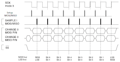
SPI MODE 3:
          CHANGE DATA @ NEGEDGE
          read data @posedge
The SPI Mode 3 waveform is
SPI Slave verilog code

We have seen the working of SPI and the SPI Master in the previous page. Now let us see about the SPI Slave.


Click here to goto SPI MASTER Page.


SPI SLAVE VERILOG MODULE:
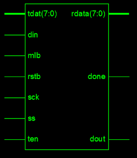
       The slave module is simple.  It is just like a shift register with additional control signal SS_bar. The data is sampled in at positive edge of SCK and shifted out at negative edge of SCK. The data transmission of slave is active only when SS_bar input signal is low, otherwise it is disconnected from the bus & Sdout is tri-stated. Other control signals are similar to that of SPI Master Module.

SPI Slave Block Diagram is


SPI Slave verilog code


The SPI Slave module verilog code is as follows:
//read from  sdin
always @(posedge sck or negedge rstb)
  begin
    if (rstb==0)
        begin rreg = 8'h00;  rdata = 8'h00; done = 0; nb = 0; end   //
    else if (!ss) begin
            if(mlb==0) 
                begin rreg ={sdin,rreg[7:1]}; end
            else    
                begin rreg ={rreg[6:0],sdin}; end 
            nb=nb+1;
            if(nb!=8) done=0;
            else  begin rdata=rreg; done=1; nb=0; end
        end
  end


//send to  sdout
always @(negedge sck or negedge rstb)
  begin
    if (rstb==0)
        begin treg = 8'hFF; end
    else begin
        if(!ss) begin           
            if(nb==0) treg=tdata;
            else begin
               if(mlb==0)
                    begin treg = {1'b1,treg[7:1]}; end
               else 
                    begin treg = {treg[6:0],1'b1}; end           
            end
        end //!ss
     end //rstb   
  end //always


SPI Slave verilog code output


Click here to goto SPI MASTER Page.


If you enjoyed this post plz let us know your views via comments.
This helps us to do much more better.
Thankyou.

Search Here...